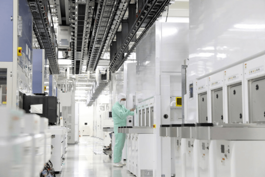
The center of gravity in semiconductors is shifting.
For years, the market treated frontend process technology as the main source of competitive advantage. But in the AI era, that is no longer enough. Once GPUs become larger, HBM stacks get taller, and package-level integration becomes more complex, the real performance bottleneck starts moving into packaging, bonding, dicing, and testing. That is why backend processing is now moving from a supporting role to a strategic one. TSMC’s advanced packaging remains a visible bottleneck in 2026, and ASE is openly forecasting a sharp expansion in advanced packaging revenue this year.
1. Why backend processing has become stronger
The reason is simple.
As AI chips and HBM scale up, packaging begins to determine performance itself. Compute alone no longer defines system value. What matters now is how efficiently dies are connected, how much heat can be managed, how reliably ultra-thin wafers can be handled, and how much yield can be preserved through increasingly fragile processes. Broadcom said in March that TSMC capacity had become a supply bottleneck in 2026, and specifically pointed to advanced packaging constraints as part of the problem.
That is why this cycle looks different from older semiconductor upcycles.
The critical bottleneck is no longer only lithography. It is increasingly the set of backend steps that make advanced AI chips manufacturable at scale. ASE’s guidance that its advanced packaging business will double to about $3.2 billion in 2026 is one of the clearest signs of that shift.
2. The first major beneficiary: bonding equipment
The first big winner in backend processing is bonding.
As HBM stacks get taller, the question becomes how precisely the layers can be attached. Traditional thermal-compression approaches still dominate, but once the industry moves toward 16-layer and 20-layer-class stacking, package height and thermal resistance become much more difficult constraints. That is exactly why hybrid bonding is drawing so much attention. Applied Materials says its Integrated Hybrid Bonding system was designed to enable direct copper-to-copper chip connections with much shorter interconnect length, lower resistance, and much higher I/O density than microbump-based approaches.
Within hybrid bonding, the most important distinction is W2W versus D2W.
W2W still has scale advantages, but D2W is increasingly seen as more favorable when yield protection matters because only known-good dies can be selected and stacked. Recent industry analysis described W2W as the current mainstream approach, while highlighting D2W as the faster-growing segment. That is why the market is paying close attention to players such as Besi, Applied Materials/Kinex, Hanmi Semiconductor, Hanwha Semitech, and Semes. Korean media also reported that SK hynix has been building a hybrid bonding pilot line using AMAT’s Kinex system while competition among Besi, Semes, and Hanwha Semitech intensifies.
3. The second major beneficiary: dicing equipment
The second key area is dicing.
As wafers become thinner, cutting technology has to evolve with them. Older blade-based approaches were workable for thicker wafers. Laser dicing became more useful as wafers thinned. But with next-generation HBM and advanced logic, the market is increasingly moving toward more precise low-damage methods, including ultrashort-pulse and femtosecond laser approaches. Recent Korean coverage said local challenger ITI is promoting crack-free laser cutting specifically for HBM4 and glass-based applications, underscoring how important thin-wafer damage control has become.
This matters because HBM4 is pushing the manufacturing envelope.
SK hynix has already shown 16-layer HBM4, and TrendForce reported the company is exploring tighter die spacing and new packaging methods to improve HBM4 stability under severe thickness constraints. Excessive thinning increases vulnerability to shock and handling damage, which is exactly why the dicing process becomes more strategically important.
So the dicing story is not just about memory.
It is increasingly relevant across advanced logic, advanced packaging, and glass-substrate-adjacent roadmaps too.
4. The third major beneficiary: inspection equipment
The third major winner is inspection and test.
As process complexity rises, yield becomes more valuable than ever. A defect at advanced nodes or inside an expensive AI package causes far more damage than it used to. Industry price estimates in 2026 still place 28nm 300mm wafers around $3,000, while 5nm wafers are often cited in the $16,000–$18,500 range, which means the financial cost of a missed defect is dramatically higher than it was in earlier generations.
That is why inspection is no longer optional insurance.
The more complicated the process flow becomes, the more the market needs step-by-step verification. That includes EDS at wafer level, followed by package test, burn-in, and module-level validation in later stages. In advanced AI packaging, inspection is not just a quality tool. It is a direct lever on profit protection.
5. Foundry recovery and the OSAT market need to be separated
The final point is important.
Investors should not treat memory and non-memory backend demand as if they are driven by the same logic. In memory, the story is HBM stacking, thinning, bonding, and yield. In foundry and logic, the story is advanced packaging, CoWoS-style integration, AI accelerators, and HPC-linked package complexity. These are related, but not identical. NVIDIA has already said its advanced packaging needs are changing rather than shrinking, and Jensen Huang made clear last year that packaging constraints were still a bottleneck even as the product mix evolved from CoWoS-S toward CoWoS-L.
That is why backend exposure has to be read in layers.
If TSMC remains capacity constrained, Samsung Foundry can gain strategic value as an alternative for some customers. And when AI and HPC demand increases, the spillover often appears not only in wafers, but also in non-memory test and packaging volumes. That is one reason ASE is seeing such a sharp advanced-packaging ramp, and one reason memory OSAT pricing has reportedly jumped by as much as 30% in certain segments.
The real message is simple.
In the AI era, frontend still matters.
But backend is where the next battle for performance, yield, and monetization is increasingly being fought.

댓글 남기기